GaN 에피택셜 웨이퍼
(68)
Fe는 GaN 기판 Resistivity > 106 Ω·Cm RF 장치에게 도핑했습니다
가격: Negotiable
MOQ: Negotiable
배달 시간: 3-4 week days
상표: GaNova
하이 라이트:ISO GaN Substrates, gan semiconductor wafer, Fe Doped GaN Substrates
2inch C-face Fe-doped SI-type free-standing GaN single crystal substrate Resistivity > 106 Ω·cm RF devices The achieved breakdown voltage of the Fe-doped GaN epitaxial layer can be as high as 2457 V, which is attributed to the Fe-doped GaN epitaxial layer with higher resistance, which can sustain... 더보기
지금 연락하세요
원문대로 에피택셜 웨이퍼
(42)
4 인치 4H-SiC 기판 P 레벨 SI 500.0±25.0μm MPD≤5/cm2 저항성≥1E5Ω·cm 전력 마이크로 웨이브
가격: Negotiable
MOQ: Negotiable
배달 시간: 3-4 week days
상표: GaNova
하이 라이트:P 레벨 4H-SiC 기판, 마이크로웨이브 4H-SiC 기판, 4인치 4H-SiC 기판
전력과 마이크로파 소자를 위한 JDCD03-002-002 4 인치 4H-SiC 기판 피-준위 SI 500.0±25.0μm MPD≤5/cm2 Resistivity≥1E5Ω·cm
개관
SiC는 다이오드와 파워 트랜지스터와 고전력 마이크로파 소자와 같은 매우 고전압과 고전력 장치의 제작을 위해 사용됩니다. 전통적 Si 장치와 비교하여, SiC-기반을 둔 전력 소자는 더 빨리 고온 능력 때문에 요구한 교환 속도 더 높은 전압, 더 낮은 저항 성분, 더 작은 크기, 더 적은 냉각을 가집니다.
... 더보기
지금 연락하세요
GaAs 에피 웨이퍼
(15)
JDCD10-001-003 2인치 GaAs ((100) Zn 도핑 기판
가격: Negotiable
MOQ: Negotiable
배달 시간: 3-4 week days
상표: GaNova
하이 라이트:2인치 Zn 도핑 기판, 2인치 Zn-Doped Substrate
2인치 GaAs(100) Zn 도핑 기판
개요GaAs Wafer의 Gallium arsenide는 전기로부터 직접적인 방식으로 레이저 광을 발생시키는 특성을 갖는다.GaAs 웨이퍼에는 두 가지 유형이 있습니다.다결정 및 단결정.이 웨이퍼는 LED, 마이크로웨이브 회로 및 LD를 만들기 위해 마이크로 전자 및 광전자 생산에 활용됩니다.
GaAs-Zn 웨이퍼
성장 방법
VGF
행동 유형
SCN
도펀트
GaAs-Zn... 더보기
지금 연락하세요
CVD 다이아몬드 기판
(15)
XRD
가격: Negotiable
MOQ: Negotiable
배달 시간: 3-4 week days
상표: GaNova
하이 라이트:Electronic Grade Single Crystal Diamond, Electronic Diamond Substrates, Heat Sink Single Crystal Diamond
XRD 더보기
지금 연락하세요
급속 열 처리 시스템
(2)
부스트 프로덕션 급속한 열처리 RTP-SA-8 앙일링 시스템
가격: Negotiable
MOQ: Negotiable
배달 시간: 3 month
상표: Ganova
하이 라이트:Boost Production Rapid Thermal Processing, Rapid Thermal Processing Annealing System
1.Basic configuration of equipment system 1.1outline The Rapid Thermal Processing is a vertical semi-automatic 8-inch wafer rapid annealing furnace, which uses two layers of infrared halogen lamps as heat sources for heating. The internal quartz cavity is insulated and insulated, and the outer shell... 더보기
지금 연락하세요
홀 효과 센서 테스터
(3)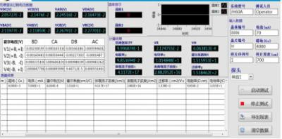
Hall Coefficient Hall Effect Sensor Tester Mobility Resistivity Measurement
가격: Negotiable
MOQ: 1
배달 시간: 8-10week days
상표: GaNova
하이 라이트:Hall Effect Sensor Tester Mobility Resistivity, carrier concentration hall effect instrument, Hall Effect Sensor Tester semiconductor
Hall Coefficient Hall Effect Sensor Tester mobility resistivity measurement Product Overview: Hall effect tester is used to measure the carrier concentration, mobility, resistivity, Hall coefficient and other important parameters, and these parameters of semiconductor materials to understand the ele... 더보기
지금 연락하세요
알루미늄 질화물 웨이퍼
(21)
JDWY01-001-007 2인치 후막 (4,5) 사파이어 웨이퍼 상의 Um AIN, SSP, XRD FWHM Of(002)≤160arcsec\(102) ≤400arcsec
가격: Negotiable
MOQ: Negotiable
배달 시간: Negotiable
상표: GaNova
하이 라이트:SSP AIN On Sapphire Wafer
사파이어 웨이퍼의 2인치 후막 (4,5)um AIN, SSP, XRD FWHM of(002)≤160arcsec(102) ≤400arcsec UV 소독, LED 칩
사파이어는 물리적, 화학적, 광학적 특성이 독특하게 조합된 소재로 고온, 열충격, 물과 모래 침식, 긁힘에 강합니다.
안건
AlN-TCU-C50
치수
φ50.8 mm±0.1 mm, OF(1-100), Al Face, 위치 결정 에지 16.0± 1.0 mm
기질
사파이어(단면 또는 양면 광택 처리... 더보기
지금 연락하세요
레이저다이오드 칩
(10)
94um Laser Diode Chip Slope Efficiency 1.0W/A Wavelength 915nm
가격: Negotiable
MOQ: Negotiable
배달 시간: Negotiable
상표: GaNova
하이 라이트:94um Laser Diode Chip, high power laser diode chip, 1.0W/A Laser Diode Chip
94μm Laser Diode Chip Slope Efficiency 1.0W/A Wavelength 915nm 915nm 10W COS Diode Laser Chip On Submount Design For low power consumption it is essential that the output from the laser diode (LD) is efficiently coupled to the optical waveguide, and there are several approaches reported in the liter... 더보기
지금 연락하세요
탄화 규소 결정
(12)
JDZJ01-001-006 SiC 씨 크리스탈 S 등급 6" Φ153±0.5mm
가격: Negotiable
MOQ: Negotiable
배달 시간: 3-4 week days
하이 라이트:6" SiC 씨 크리스탈, S급 SiC 씨 크리스탈, φ153±0.5mm SiC 씨 크리스탈
sic 결정핵 S 등급 6 " S 등급 φ153±0.5mm
SiC는 애벌런치 항복을 겪지 않고 Si 또는 GAA 보다 더 큰 8 번 동안 전압 물매 (또는 전기장에) 견딜 수 있습니다. 이 높은 파괴전계는 고전력 마이크로파 소자와 더불어, 다이오드, 전력 트랜지스터, 파워 다이리스터와 서지 흡수기들과 같은 매우 하이-볼타게, 고전력 장치의 제작을 가능하게 합니다. 덧붙여, 그것은 매우 위치되기 위한 장치가 집적 회로에게 높은 디바이스 기록 밀도를 제공하면서, 함께 마감되도록 허락합니다.
등급
... 더보기
지금 연락하세요
Ga2O3 웨이퍼
(13)
JDCD04-001-007 10x10mm2(010)Sn 도핑 독립형 Ga2O3 단결정 기판 제품 등급 단일 연마
가격: Negotiable
MOQ: Negotiable
배달 시간: 3-4 week days
상표: GaNova
하이 라이트:독립적인 Ga2O3 단일 크리스탈 기판, 제품 등급 Ga2O3 단일 결정 기판, 10x10mm2 Ga2O3 단일 크리스탈 기판
10x10mm2(010)Sn 도핑 독립형 Ga2O3 단결정 기판 제품 등급 단일 연마 두께 0.6~0.8mm FWHM<350arcsec,Ra≤0.5nm 저항 1.53E+18Ω/cm-3 광전자 소자, 반도체 재료의 절연층 및 UV 필터
실리콘 기반 장치는 상대적으로 효율적인 장치를 생산할 수 있었지만 질화 갈륨의 향상된 특성으로 인해 GaN 반도체는 열에 훨씬 적은 에너지를 잃는 이점이 있습니다.넓은 밴드갭 덕분에 GaN 장치는 실리콘보다 훨씬 더 높은 온도를 유지할 수 있으므로 즐겨 사용하는 장치에 전반적으로 더 높은 ... 더보기
지금 연락하세요
실리콘 웨이퍼
(26)
JDCD07-001-004 MEMS 처리용 7 인치 SOI 에피타시얼 웨이퍼
가격: Negotiable
MOQ: 1
배달 시간: 3-4 week days
상표: GaNova
하이 라이트:7 인치 SOI 에피타시얼 웨이퍼, MEMS 처리 SOI 에피타시얼 웨이퍼, SOI 에피타시얼 웨이퍼
MEMS 공정용 7인치 SOI 에피택셜 웨이퍼
개요실리콘 웨이퍼는 우리의 삶을 풍요롭게 하는 각종 전자제품에 들어가는 반도체 제조에 꼭 필요한 소재입니다.일상에서 실제 실리콘 웨이퍼를 접할 기회가 있는 사람은 거의 없습니다.실리콘 웨이퍼는 모양이 원형인 실리콘 결정으로 구성된 재료와 같은 결정 반도체의 얇은 조각입니다.
사양
소이
지름
4''
5''
6''
7''
장치 계층
도펀트
붕소, 포... 더보기
지금 연락하세요
사파이어 웨이퍼
(19)
JDCD08-001-006 6 인치 씨 플레인 사파이어 기판 웨이퍼
가격: Negotiable
MOQ: Negotiable
배달 시간: Negotiable
하이 라이트:6inch Sapphire Substrate Wafer
JDCD08-001-006 6 인치 씨 플레인 사파이어 기판 웨이퍼
사파이어는 내구성에 다이아몬드로 유일한 두번째입니다다이아몬드는 도대체 가장 오래가는 자연스럽게 발생 요소이고, 광물 견고성의 모스 경도계에 10 / 10으로 랭크됩니다. 사파이어는 또한 매우 오래가고, 모스 경도계에 9 / 10으로 랭크됩니다.
거의 온라인 소스들로부터 그리고 전통적 소매 점포에서 모든 사파이어와 사파이어 빛 보석은 적격자로 묘사됩니다.
6 인치 씨 플레인 고순도 Al2O3 기판
... 더보기
지금 연락하세요
무늬가 있는 사파이어 기판
(10)
UKAS Patterned Sapphire Substrates Flat Edge Angle
가격: Negotiable
MOQ: 1
배달 시간: Negotiable
상표: GaNova
하이 라이트:UKAS Patterned Sapphire Substrates, al2o3 substrate 430um, Patterned Sapphire Substrates OEM
50.80±0.10mm Patterned Sapphire Substrates Flat Edge Angle A-Plane±0.2o 2inch Patterned Sapphire Substrates,LED Chip,Substrate Material The efficacy enhancement of GaN-based LEDs with the patterned-sapphire substrate technique is generally attributed to the improvement in both light extraction effic... 더보기
지금 연락하세요
테플론 웨이퍼 홀더
(1)
꽃 바구니와 손잡이를 청소하는 6inch 테플론 웨이퍼 홀더
가격: Negotiable
MOQ: 1
배달 시간: Negotiable
하이 라이트:6inch Wafer Holder, wafer cassette carrier, 25 PCS Wafer Holder
6inch Wafer Holder Cleaning Flower Baskets And Handles PFA Cassette / Cassette of wafer can be customized and designed by customers’ request, able to resist strong acid, strong hydrofluoric acid, strong base and heat up to 200~220℃, use to deliver wafers in acid & base process of Fabrication f... 더보기
지금 연락하세요
웨이퍼 다이싱 머신
(5)
0.1mm/s To 600mm/s Wafer Dicing Machine X Axis Cutting Range 260mm
가격: Negotiable
MOQ: 1
배달 시간: 8-10week days
상표: GaNova
하이 라이트:0.1mm/s Wafer Dicing Machine, wafer saw machine 260mm, 600mm/s Wafer Dicing Machine
DAD3350 Wafer Dicing Machine 0.1 ~ 600mm/s X-Axis Cutting Range 260mm Improved throughput The DAD3350 achieves improvement in throughput by increasing the speed of each axis. Ease of use Operability is improved with installation of an LCD touch screen and Graphical User Interface (GUI). Easy operati... 더보기
지금 연락하세요